Rapberry PI compute module 4 NAS PCB for using JLCPCB.com. (pre-test version)
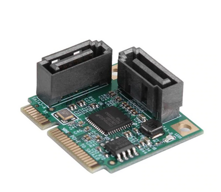
Main purpose of design is to make NAS with more reliable SATA connection comparing to USB-to-SATA converters. SATA controllers can be connected through MiniPCIe slot. There are variety of cards in market, mainly my intend was to use this for 2 SATA (see picture below). This is half size card. Cards for 4 SATA with RAID controller also can be connected.
Design is made using nighly version of KiCAD 5.99.0 Please study Raspberry PI CM4 datasheet
PCB was designed by a newcomer. All steps made are listed below. This section is very important and risky. Mistakes can be made. 90 R and 100R impedance differential lines are used.Calculations of differential lines are made using JLCPCB internal calculator
Results of calculation - 90R and 100R
Those results put in KiCAD.
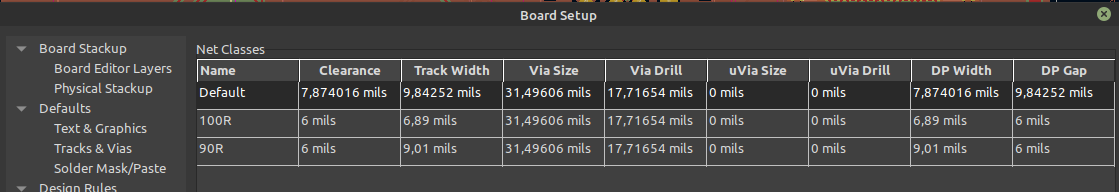
JLC7628 Stackup used all settings transfered to KiCAD stackup
All vias minimal diameter is 0.45 as price will be much higher for VIAs of less size.
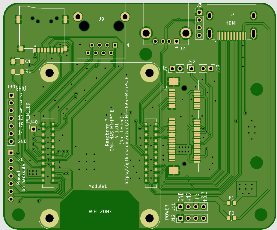
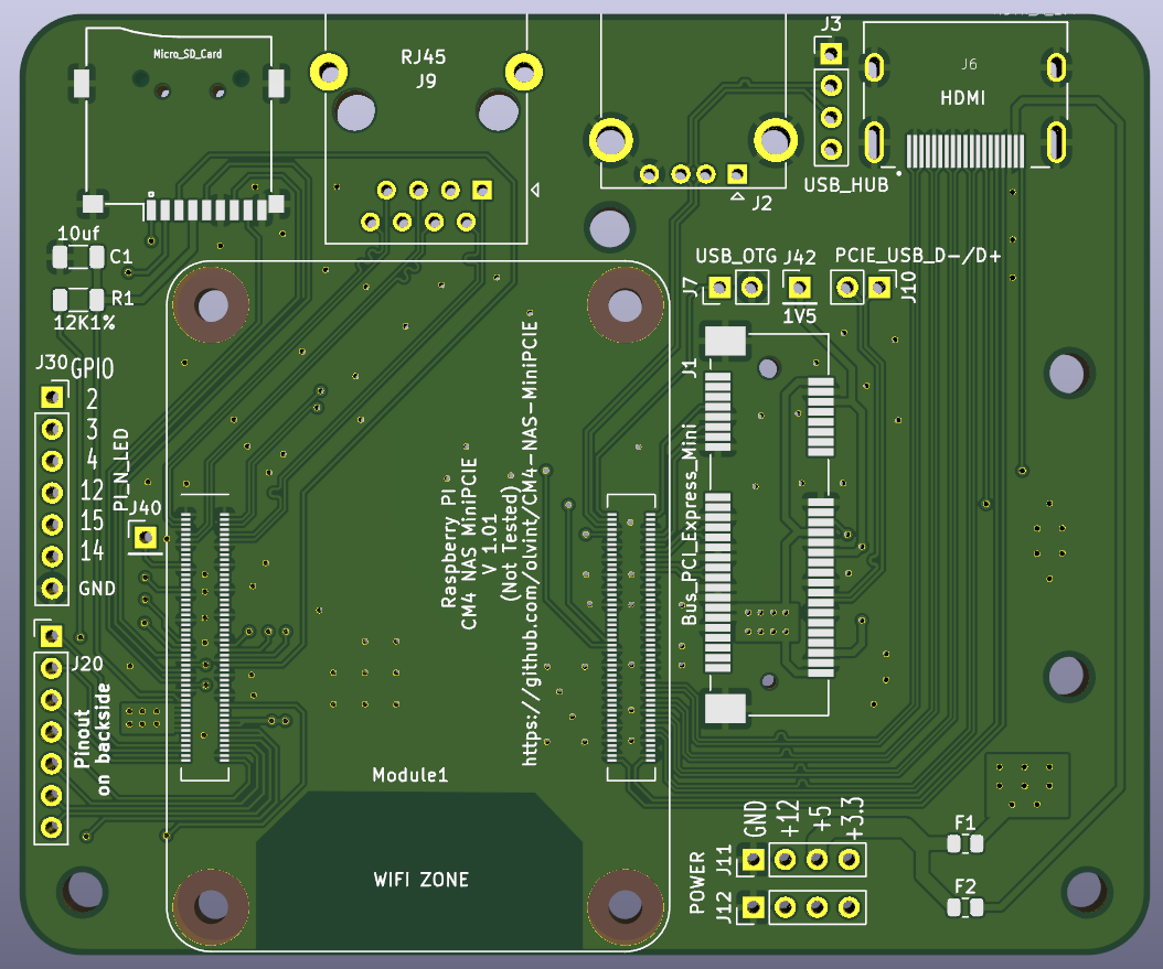
- MiniPCIe slot (designed for hlaf-size cards)
- HDMI in order to use device as media player
- Gigabit LAN
- SD card slot for using CM4’s without eMMC
- USB A 2.0 socket for connecting periphery like Zigbee.
- MicroUSB for installing firmware to CM4 and power supply. All sockets placed on top edge of PCB for more reliable use and easy design of 3D print case.
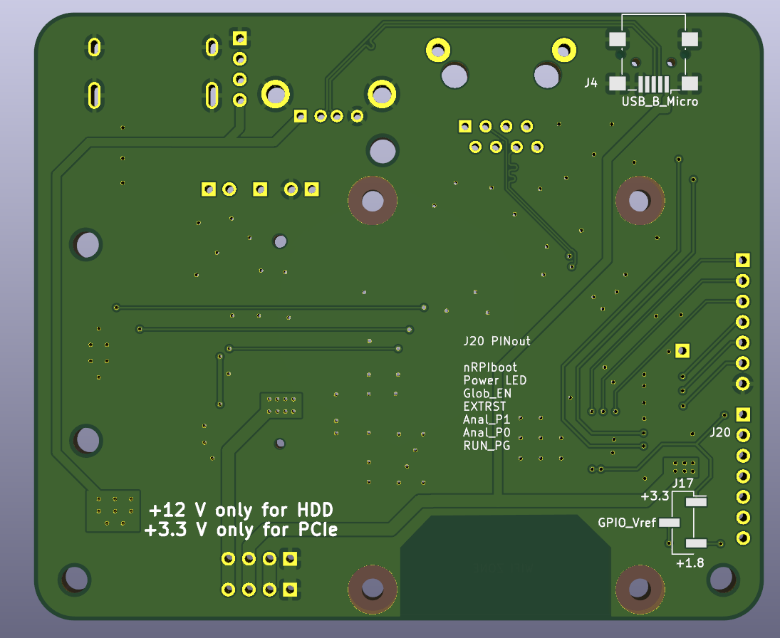
All sockets footprints selected to be most common. In standard library of KiCAD I did not found suitable MicroSD socket. And ofcource footprint of CM4 is also taken from Raspberry PI CM4 IO borad. All external footprints are in folder LIBS. I wanted to install all sockets on one side of the board and there was not much space. MicroUSB socket I put on other side of the board below MicroSD socket.
There are 2 connectors with 4 pins (GND, +12V, +5V, +3.3V) Connectors can be used for powering board and soldering cable for powering HDDs.
- +12 V is only used for HDD. Board has 2 interconnected pins, but level +12 V not used on board. MiniPCIe does not have +12V input.
- +5V used for powering CM4 module and giving power to USB and HDMI. Two SMD resettable fuses installed to protect board from short circuit.
- +3.3 V used for powering PCI-to-SATA module. Nothing else.
- 1.5 V. Special connector made above PCIe slot. Generaly this level is not required. It is planned to use SATA module based on chip ASM1061 that has Integrated 3.3V to 1.2V switch regulator.
Initial CM4 IO Borad has more copmplicated power system with different ICs for protecting not only from short circuit but, under voltage, overload etc.
Left side of board has GPIO connector and small connector for selecting level of GPIO (GPIO_Vref)
- GPIO 2
- GPIO 3
- GPIO 4
- GPIO 12
- GPIO 15
- GPIO 14
There is a connector with following signals
- nRPIBOOT
- PI_POWER_LED
- Global_EN
- nEXTRST
- Analog_P1
- Analog_P0
- RUN_PG
- PI_N_LED
- USG_OTG connector used to connect USB_OTG_ID pin of CM4 for installing firmware to eMMC.
- USB hub connecor Connector with 4 pins GND, D+, D-, +5V can be used to connect external USB hub if you need it in your project.
- MiniPCIe USB D+/D-. MiniPCIe slot also has connections for D+ and D- another connector used for it. This is not connected to CM4 D+/D- lines.
- One GND connector just for the case.
GBR files are prepared in FAB folder. Also archive prepared FAB_JLCPCB.zip for making order. Please note that you need to turn on option Impedance and select JLCPCB7628 stackup
Front
Back
Update 28.12.2020 - Rerouted some tracks. Moved MicroUSB below MicroSD. Update 02.01.2021 - Rerouted a lot of tracks. Added beauty.