-
Notifications
You must be signed in to change notification settings - Fork 53
build it
- BOM (for rev 1.c, rev1.b, rev1)
- note this doesn't include part #s for the breakable, round/machine pin headers and sockets. re knobs: options include sifam (w/ "encoder caps"), rogan 2s, and cliff K85 (+ suitable cap).
-
jumpers high-lighted (in blue), red: ignore/don't populate:
- silkscreen (rev 1c)
- silkscreen (rev 1b) (pictured above)
- silkscreen (rev 1)
-
in case of doubt, check the change log.
-
generally speaking, it's a very easy + quick build. you can follow the values printed on the board, except:
-
ignore the pads labelled
29, and (if present)79L05andLM4040-3; none of this is required. theLM4040-5is required.
-
ignore the pads labelled
-
if you have a pre-rev.1b PCB, as per BOM use 100k where it says 49k9 (around the MCP6004): see below.
-
other than that, no particular precautions. that said, make sure to look at the notes below re:
- OLED pins/aluminium panels (these shouldn't touch !).
- jumper(s).
-
using the default resistor values, the DAC output will be roughly bipolar, 9VPP swinging around 0V (-4.5V / 4.5V). that's a vestige, kind of, from when i planned to add LFOs etc (which i didn't). so, if you'd prefer a more positive output range (output #4 is used a clock output, after all, most of the time / in most modes), you'll have to change the offset. to do this, swap the
3k9resistor — the one above the NPN transistors (nearby a/the 470n cap) — for10k; this will shift up the range to -2V / 7.25V. ie, this one: -
note: if you do this, the code, which defaults to bipolar, doesn't know. you'll have to re-compile the code with
#define MOD_OFFSET(in TU_options.h).
-
this is how things should look with the all the parts installed. note the socket for the teensy with extra hole for the DAC pin (1x14 + 1x14 + 1 extra pin):
-
pin header labelled
clk/DAC: connect the two pins where it saysDAC, ie the middle and top-most hole (cf picture above). -
the second jumper (simply use wire) goes between the square pin and the middle pin (NB: jumper entirely removed in rev 1c, so don't worry about it).
-
the jacks share the ground pad, facing each other:
-
NB: previous PCB revisions had holes that were too small for the lugs; in case you have such a PCB, just snip off the lugs:
-
rev1.c has wider holes, so the encoders will fit just fine:
-
either way you'll need a bunch of washers so that things line up nicely with the jacks.
-
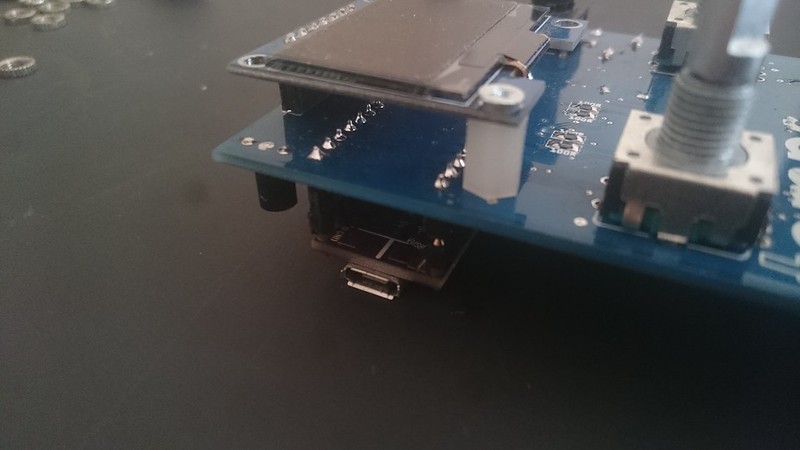
use a low profile socket. you'll have to trim the pins somewhat (or replace the header) so as to make things fit / line up with the other components (ie jacks, encoders):
-
if your OLED refuses to sit properly, a suitably sized spacer (~ 6mm) will help:
-
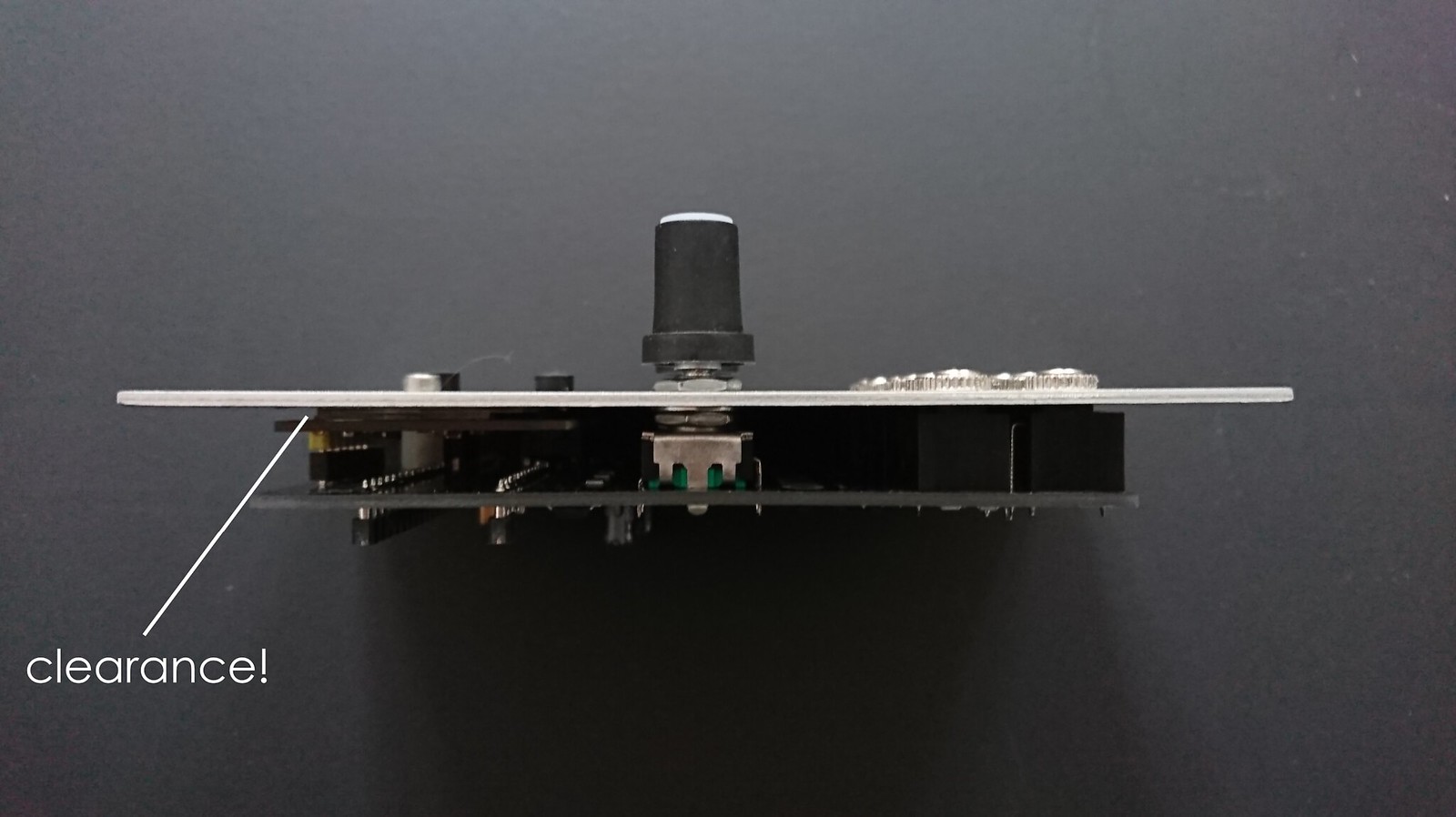
if using an aluminium panel, make sure the OLED pins don't touch the panel! (ie cut them flush with the pcb)!
-
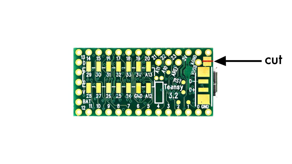
you have to cut one trace, to separate V_USB and the external/eurorack PSU. this is the trace:
-
PCB versions prior to version rev.1b: these lack a suitable external pull-up to override the LED, so the onboard teensy SMD LED needs to be removed for right encoder switch to work properly. in most recent versions, the
10kresistor right next to the teensy 3v3 pin takes care of that. for older versions: don't worry, your teensy will be ok, the LED is entirely superfluous. you can easily identify the LED, it's near pin 14/A0. just snip it off with the tip of your iron. if you have a pcb labelledrev 1.borrev 1.c, this is no longer required (as noted).
-
to improve the mechanical stability, it makes sense to use a spacer (10mm, 3M) in between panel and PCB:
-
(in the picture, i cheated, because i ran out of 10mm spacers; but you get the idea).
-
with black matte PCB panel:


